

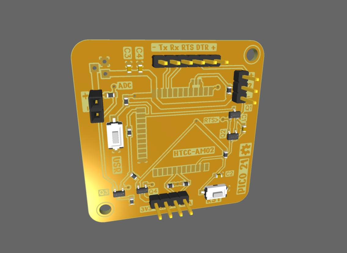
AM02 LoRa Module proto-board
Updated:
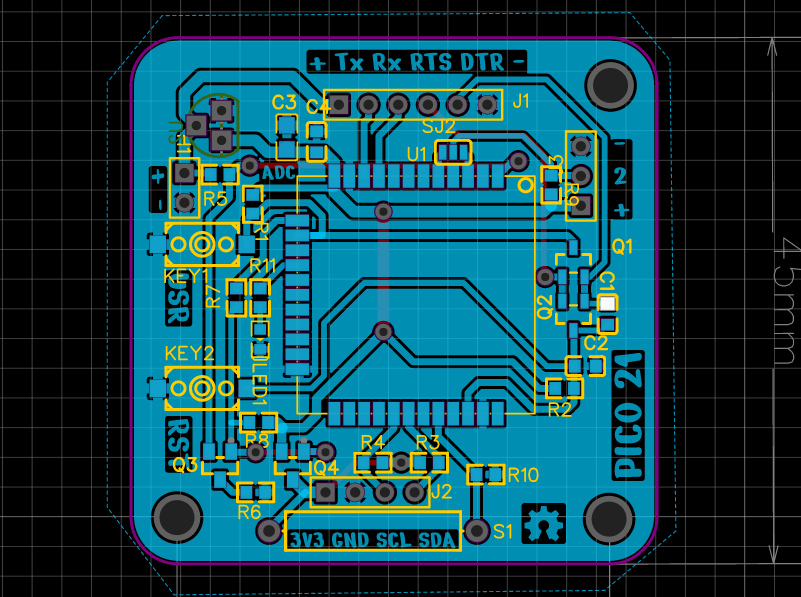
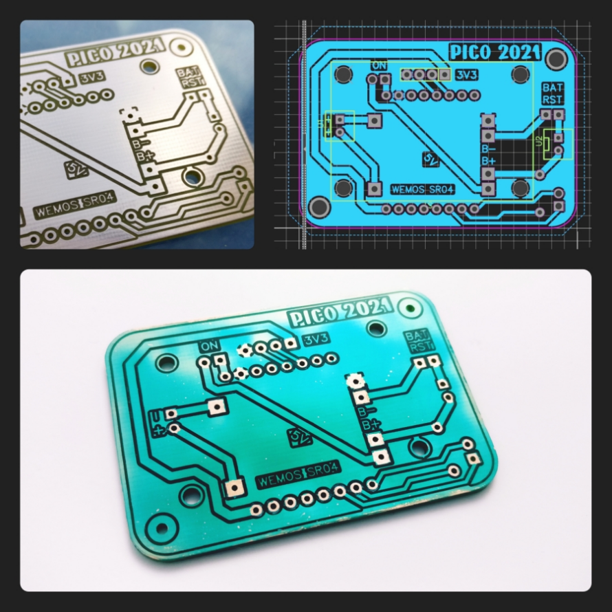
PCB design
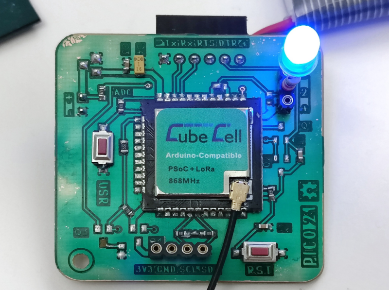
I have recently purchased some AM02 PSoC lora modules from Heltec and decided to test them embedded with a proper PCB.
The documentation for Arduino-compatible modules suggests the basic passives components for a minimal configuration, autoboot with N-channel MOSFETS, circuitry to shut down sensors during deep-sleep and battery reading via one of the 3 ACDs.
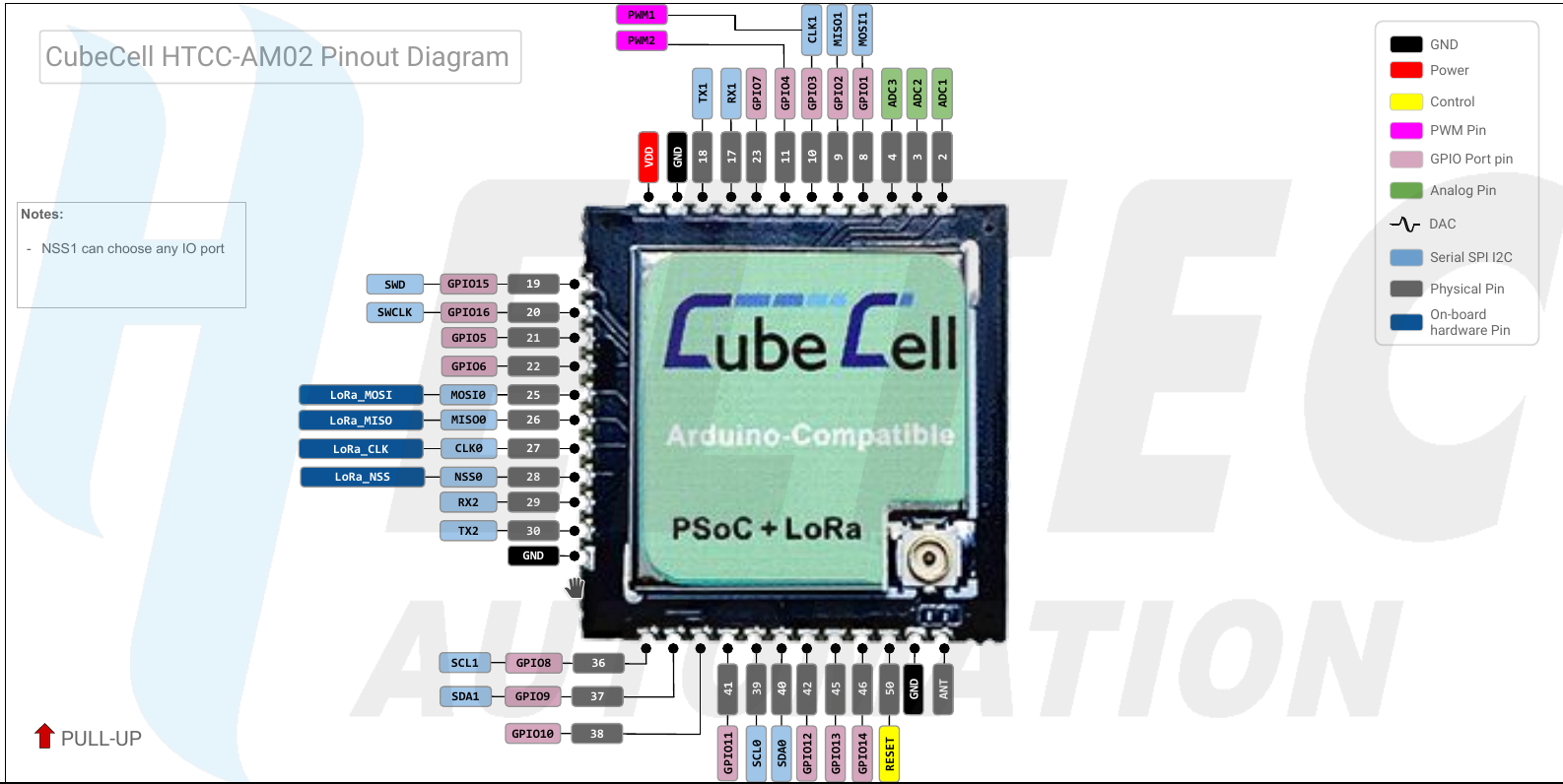
I decided to test a few GPIO, one LED, I2C, and two ADC channels.
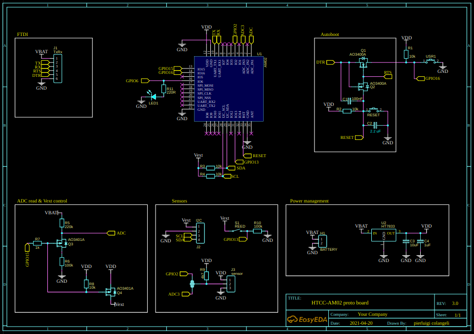
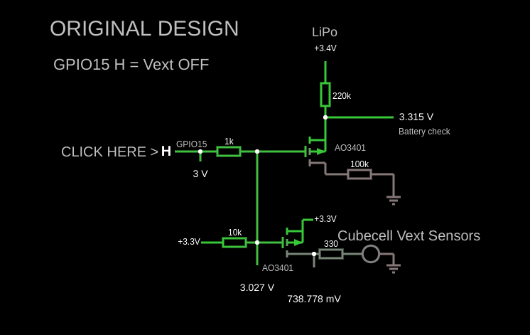
Understanding Vext and Battery check
As I’m not that familiar with MOSFET, it was very helpful to run a simulation of the Vext control. Both P-channel MOSFET are controlled by GPIO15 and have a 10k pull-up resistor tied to the gate. When GPIO15 is set to LOW, the Vext channel is open and the ADC read the battery voltage through a voltage divider (220k–V–100k). According to the Ohms Law:
Vout = Vsource * R2 / (R1 + R2)
Using a fully charged Lipo battery, this means the voltage at the ADC channel will be:
> Vadc = 4.2 * 100 / (220 +100)
> 1.3125 V
To be on the safe side, would be probably better to increase the 220k to 330k, resulting in a max readig of a bit less than 1 V.
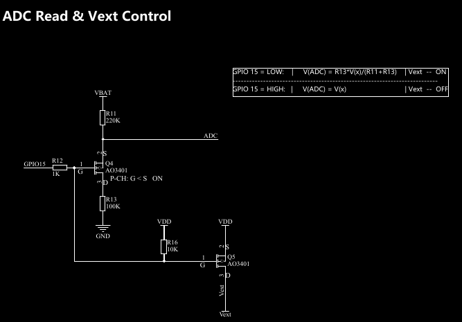
Click on the image to open up the simulation and observe the behavior of the battery check and Vext control >
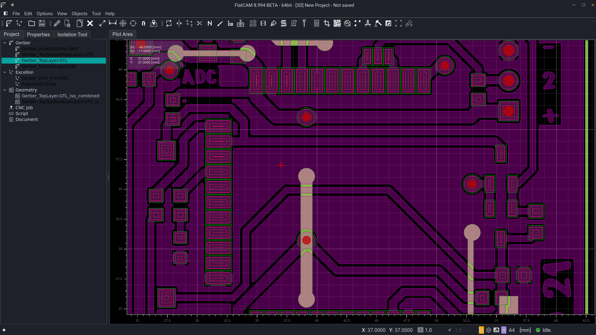
FlatCAM to gcode
FlatCAM is a great tool that digests gerber files and transform them in geometries, then in gcode. Quite some tweakings to get to the final product, but once the pipeline is established it’s easy to carve double-sided pcbs with UV mask, solder mask pads, vias and complex cutouts.
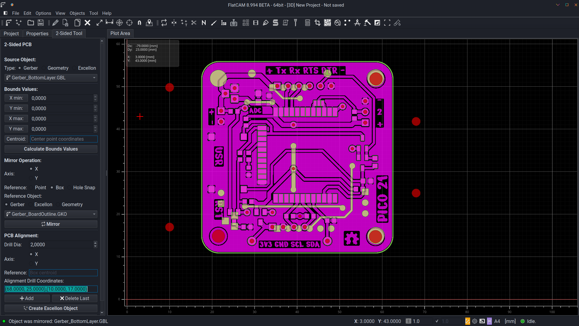
Alignment holes
Under tools, click on Double-sided PCB and select the layer you want to mirror. I mirror the bottom one on the X axis. Press Shift and click with left mouse where you want to create two of the aligment holes, FlatCAM will mirror them to make 4.
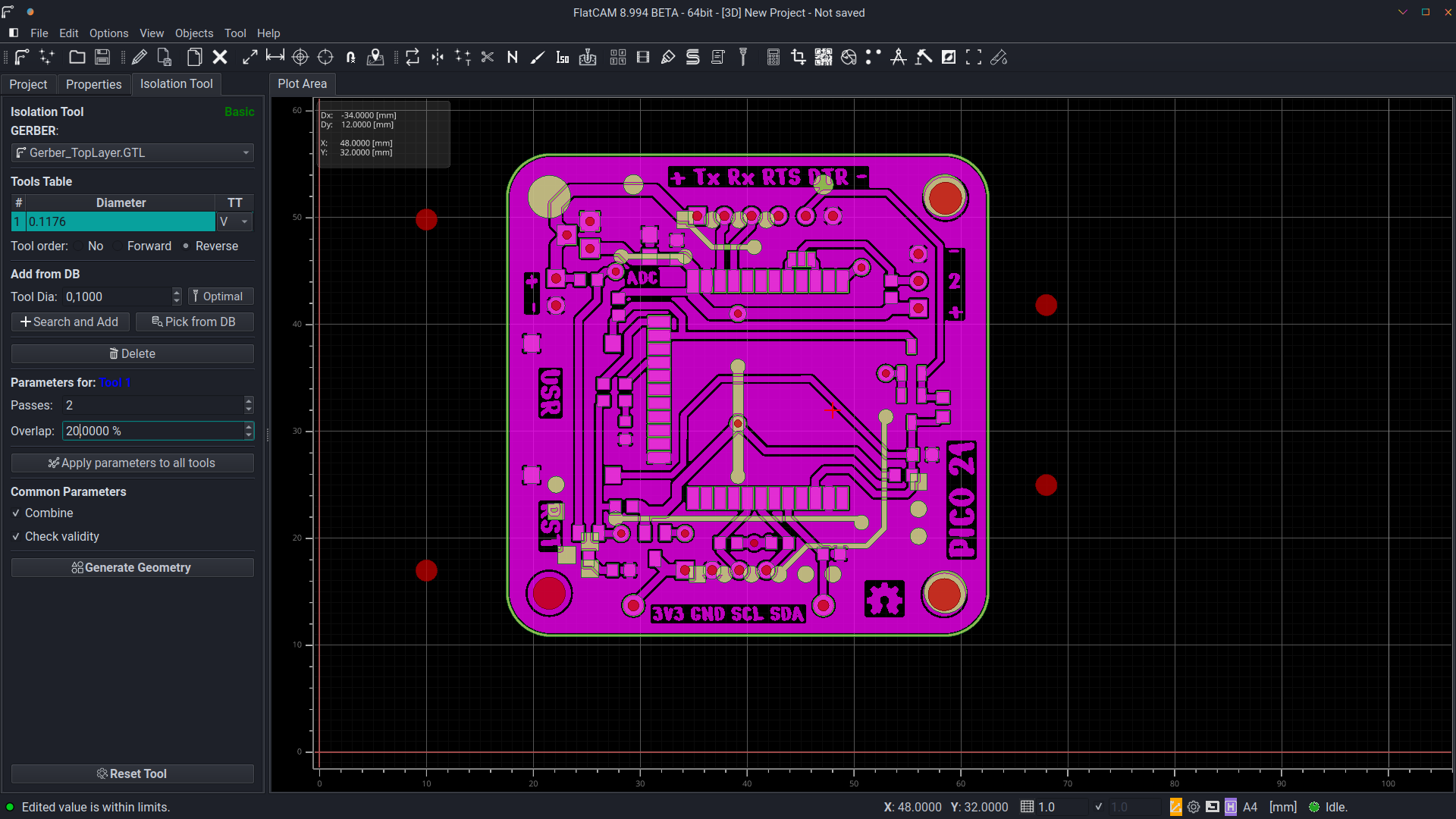
Isolation routing
For top and bottom traces I use a 20°, 0.1 mm tip diameter V shaped tool. On trace layers properties, I set the cut diameter to 0.1176 mm, this value will result in a Z = -0.05 mm, just enough to isolate traces and avoid stressing the tool with unnecessary load.
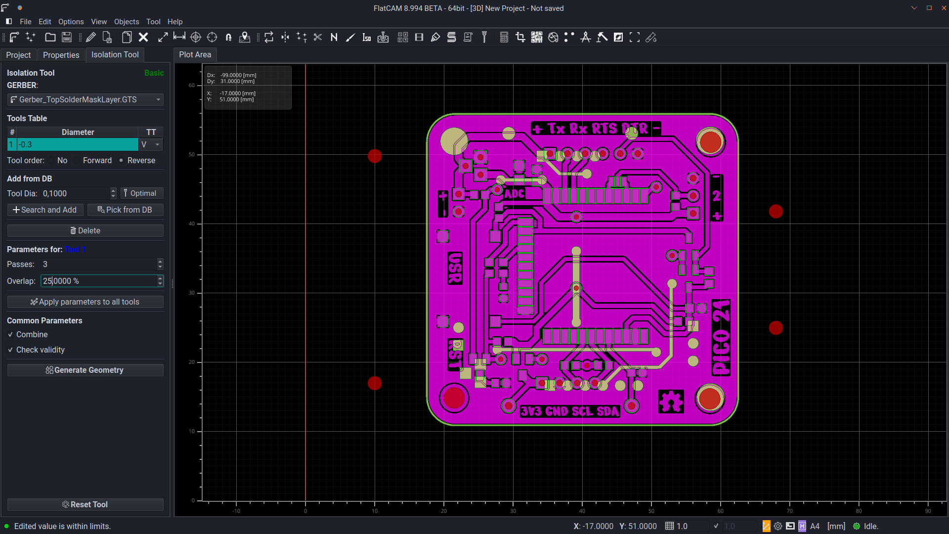
Apply UV mask and remove it from pads
I apply solder mask in two stages:
- fist pass to fill traces’ lateral channels
- solid, spread coating with transparent sheet
Expose to UV lamp for 2 minutes (depends on lamp power - trial and error). I found that a longer exposure makes the UV mask opaque and the film difficult to remove, whereas a 2 min exposure leaves the surface shiny.
In FlatCAM, I use the solder mask layer in isolation routing mode with tool diameter set at -0.3 mm. This will carve the pads internally, and not on the outside. Here you want a cut of Z = 0, just a light pass to remove the mask.
Placing small traces & ground-plane vias
In the CAD software, I set the vias drill size to 0.5 or 0.6 mm, with pad size around 1.4 mm, to be sure to have enough substrate for continuity. Just snug in some solid copper wire in the vias, and cut the exceeding portions with a sharp flat tool, then solder the extremities with plenty of flux.
First upload
#include "Arduino.h"
#define LED_BUILTIN GPIO6

// the setup function runs once when you press reset or power the board
void setup() {
  // initialize digital pin LED_BUILTIN as an output.
  pinMode(LED_BUILTIN, OUTPUT);
}

// the loop function runs over and over again forever
void loop() {
  digitalWrite(LED_BUILTIN, HIGH);   // turn the LED on (HIGH is the voltage level)
  delay(1000);                       // wait for a second
  digitalWrite(LED_BUILTIN, LOW);    // turn the LED off by making the voltage LOW
  delay(1000);                       // wait for a second
}
Donating
Please consider to support me if you find this content helpful
![]()
Leave a comment